In the rapidly evolving world of semiconductor manufacturing, precision and speed are paramount. For over 60 years, Mitutoyo has built a reputation as the leading provider of metrology solutions, offering unparalleled accuracy and efficiency across the entire semiconductor production lifecycle. We take a customer centric hands-on consultative approach to metrology solutions specification, installation and ongoing support.
Full Production Lifecycle Solutions
Front-end through back-end applications
Scroll horizontally within the table below to reveal more information.
|
Application |
Measuring Challenge |
Solution |
|---|---|---|
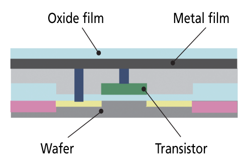
| Front End | ||
|
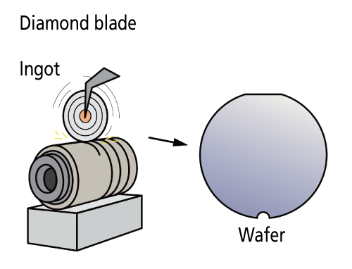
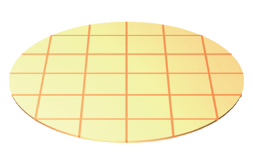
Wafer Manufacture
|
A/N Mark width, position, dot diameter, depth
Ingot Diameter
|
Automated Optical Inspection (AOI)
Laser Scan Micrometer
  |
|
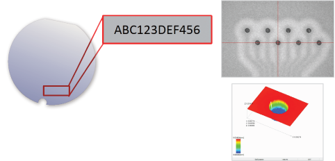
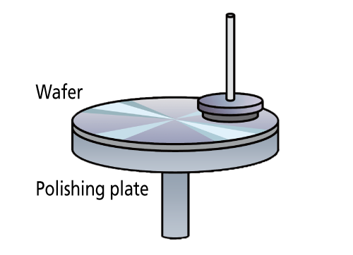
Flattening
|
Wafer thickness, back surface roughness, groove width, depth, pitch, roughness, scratches and other wafer surface defects
|
Automated Optical Inspection (AOI)
Digital Measuring Gage
Linear Encoder
Surface Roughness Measuring System
   |
|
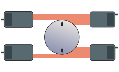
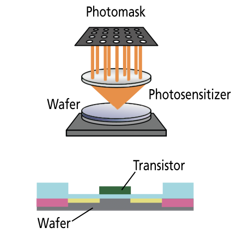
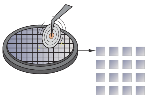
Etching
|
CVD Equipment Parts: flatness, form analysis, roughness
|
Automated Optical Inspection (AOI)
Linear Encoder
  |
|
VIA Cuts
|
Hole diameter and position
|
Automated Optical Inspection (AOI)
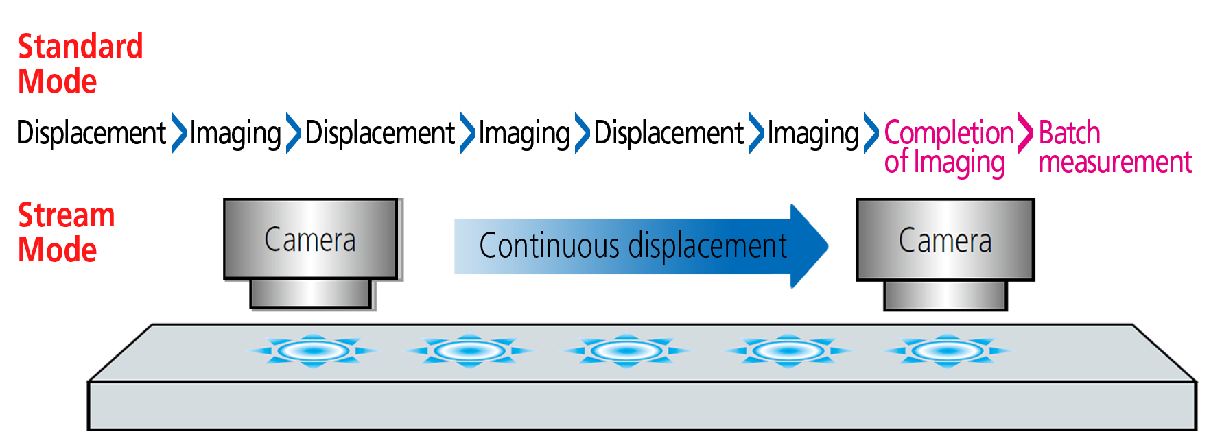
QV Apex with Stream
  |
|
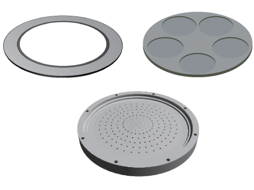
Metallization
|
Etching: electrostatic chuck, silicone ring flatness, cross section, roughness, showerhead nozzle diameter, roundness, position Sputtering
|
Automated Optical Inspection (AOI)
Coordinate Measuring Machine (CMM)
Contour Measuring System
   |
|
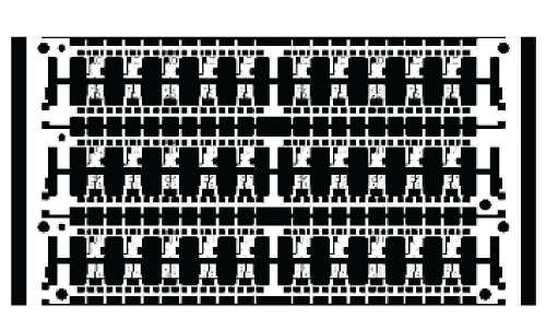
Die Sorting
|
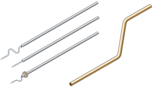
Probe card, IC test socket
Wafer probe, Probe needle
|
 Automated Optical Inspection (AOI)
Microscope
Profile Projector
|
| Back End | ||
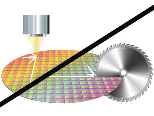
|
Dicing
|
Cross-section observation, chip thickness, post-dicing back surface burr height
|
Automated Optical Inspection (AOI)
Microscope
Ultra High Accuracy Linear Gage Probe
 |
|
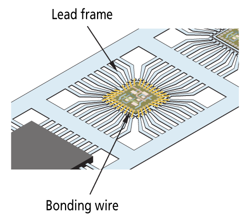
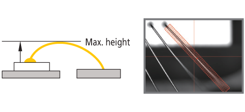
Bonding
|
Lead frame width, pitch, height, twisting
Wire loop height
|
Automated Optical Inspection (AOI)
Microscope
 |
|
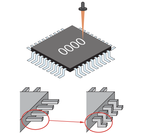
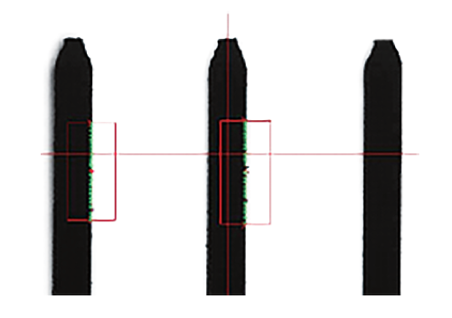
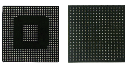
Packaging
|
Lead width, pitch, height variation, gap
Solder ball height, diameter, pitch, coplanarity
|
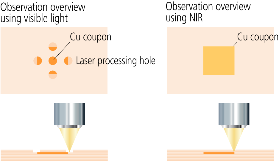
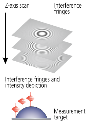
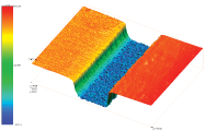
QV Hyper with WLI
Automated Optical Inspection (AOI)
Microscope
Laser Scan Micrometer
   |